A great progress in semiconductor quantum dot have been achieved by University of Science and Technology of China (USTC). Discovering the possible applications of transition metal dichalcogenides (TMDCs) in quantum chip studies, the jointed group of Professor GUO Guoping and researchers from Japanese research institutes experimentally demonstrated a fully electrotunable double quantum dot device based on semiconducting flexible 2D materials for the first time.
Combined with 2-D materials quantum dots, very small semiconductor particles, can be used to deeply investigated rich physics down to the single-particle level. Because of their outstanding electronic properties, compatibility with large-scale production, atomically thin 2-D materials, represented by graphene, expand the scope of flexible electronics and quantum electronic studies. Since the discovery of graphene in 2004, many experiments have been done on these materials. However, the band structure of graphene and impurities at interfaces and edges severely limit the performance of quantum dot devices. Up to now, quantum dot in 2D materials cannot be well controlled electrically.
Based on this background, Prof. GUO Guoping group from Key Laboratory of Quantum Information and Synergetic Innovation Center of Quantum Information & Quantum Physics of USTC collaborate with Profs. Takashi Taniguchi and Kenji Watanabe from National Institute for Material Sciences (NIMS), and Prof. Franco Nori from Institute of Physical and Chemical Research (RIKEN). They choose novel 2D material molybdenum disulfide to perform the experiments. MoS2 has a vast application prospect in quantum electronic studies, especially in spintronic and valleytronic studies which has appropriate band gap, suitable spin-orbit coupling strength and rich valley-spin physics. The joint research group use nanofabrication, low-temperature LED illumination and many semiconductor industry-level techniques, in combination with hexagonal boron nitride encapsulation technique, which has been widely used in recent 2D materials studies. With these techniques and many other efforts, they effectively reduce the impurities and disorders in the quantum dot structure, and achieve fully electrotunable double quantum dot architecture in 2D materials for the first time. At low temperatures, via tuning of gate voltages applied to the electrodes, they can tune a large quantum dot, with a width of 128 nm, into a double quantum dot, consisting of two 68-nm coupled single quantum dots. The interdot single-electron tunneling event can be tuned monotonically using the gate voltage, which means the electrically controllable evolution between artificial molecule and artificial atom is achieved. Such kind of controllable single-electron tunneling transistors provide a powerful platform to study spin-valley physics in these materials at single-particle level. Using this platform, researchers observed a physical phenomenon called Coulomb blockade weak anti-localization, indicating the effects of short-range disorders and spin-orbit couplings on electronic transport properties in MoS2.
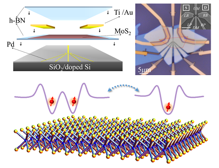
Figure. Sample images and schematics of the experiment (Image by GUO Guoping)
The results were published as “Electrotunable Artificial Molecules Based on van der Waals Heterostructures” (Science Advances 2017; 3: e1701699). Ph.D. candidate ZHANG Zhuozhi and Dr. SONG Xiangxiang from CAS Key Laboratory of Quantum Information are the co-first authors of this paper. Professor GUO Guoping and Research Associate Professor DENG Guangwei are the corresponding authors. This work is supported by the National Natural Science Foundation of China, Ministry of Science and Technology of China, Chinese Academy of Sciences, Synergetic Innovation Center of Quantum Information & Quantum Physics, and the USTC Center for Micro and Nanoscale Research and Fabrication.
The link of the paper:
Contact
Prof. GUO Guoping
pguo@ustc.edu.cn