Thanks to the perfect optical nanocavity structure and abundant coupling effects between multi-quantum states, ZnO nanowire has become an important research subject in both condensed matter physics and quantum optics, it is also one of the most promising candidates for nanoscale ultraviolet (UV) photonic and optoelectronic devices. To obtain nanoscale UV light sources with high performance, one must concurrently endow ZnO nanowire with highly-efficient band-edge emission and excellent electrical properties. However, this is impossible for those ZnO materials prepared by conventional bulk doping strategy. This is because that, on one hand, the excellent electrical properties has to be attained through dopant incorporation which can provide free carriers with the density high enough, whereas on the other hand, too much doping will inevitably suppress the band-edge emission efficiency.

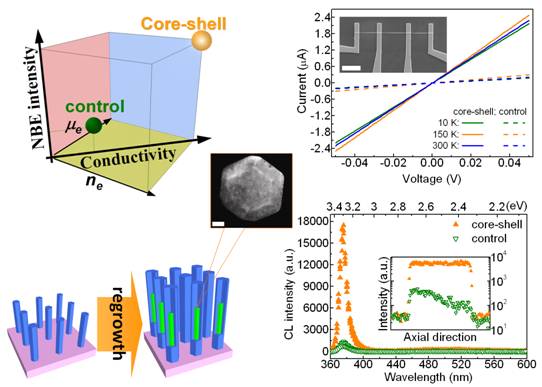
To address the aforementioned challenge, PhD student Mr. DING Huaiyi and Dr. PAN Nan of HFNL recently proposed a new strategy of nanowire interfacial doping. Through developing the CVD re-growth technique, they have produced ZnO nanowires with a unique core-interface-shell structure, whose electric conductivity surpasses 4´104 S/m, at least one order of magnitude higher than those conventional ZnO nanowires. They have found that, not only the electron concentration increases by one order of magnitude and the electron mobility improves notably, the band-edge emission intensity also enhances by at least ten fold. Further study reveals a ~3-nm-thick, Zn-rich interface layer sandwiched between the nanowire core and shell. By using the depletion and accumulation theory of semiconductors, they have proposed the mechanism responsible for the outstanding integrated performances: the interfacial Zn-doping provides the high-density free electrons, these free electrons naturally form quasi-2DEG near the interface, leading to the excellent electrical properties; furthermore, this built-in interface also serves as a barrier for the excitons’ outdiffusion, which significantly reduces the probability of the excitons diffusing to and being dissociated by the surface depletion layer, thus much increasing the band-edge emission efficiency of the excitons. This interfacial doping strategy can circumvent the intrinsic restraint of the conventional bulk doping, an intra-nanowire integration and maximization of the excellent electrical properties and high-efficiency band-edge emission can be eventually guaranteed, which is important to design and fabricate ZnO-based high-performance nano-optoelectronic devices. The results have been published in Adv. Mater. [Advanced Materials, 26(19), 3035-3041, 2014].
This work was supported by Major State Basic Research Development Programs of China, National Natural Science Foundation of China, and the Chinese Academy of Sciences.
Article link: http://onlinelibrary.wiley.com/doi/10.1002/adma.201305340/abstract
(HFNL)